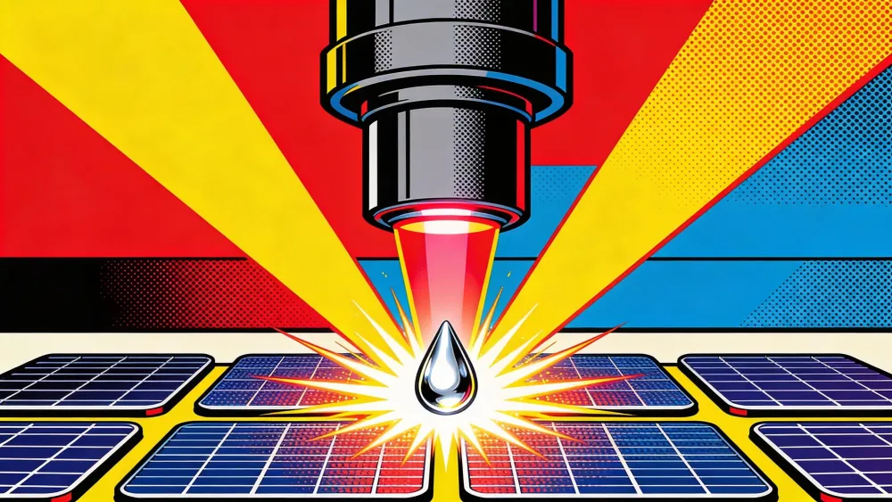
ASML told Reuters on Sunday that it pushed the extreme ultraviolet light source in its chipmaking machines to 1,000 watts. Current production systems run at 600. How? By doubling the rate of molten tin droplets fired through the machine's vacuum chamber to 100,000 per second and adding a second laser shaping burst to each one. In a production fab by 2030, that should mean 330 wafers per hour instead of today's 220. Fifty percent more chips, no new cleanrooms.
The Breakdown
- ASML boosted EUV power to 1,000W from 600W by doubling tin droplet rates and adding a second laser burst
- Wafer throughput could rise 50%, from 220 to 330 per hour by 2030, without new cleanrooms
- US startups Substrate and xLight, plus Chinese programs, race to build alternatives with hundreds of millions in funding
- ASML closed 2025 with $39.16B in sales and a $46.47B backlog, fueled by AI chip demand
Exploding tin at industrial scale
The physics are, frankly, absurd. ASML's machines fire molten tin droplets through a vacuum. Fifty thousand per second on current models. A carbon dioxide laser blasts each one, heating the tin past the surface temperature of the sun until it becomes plasma. Controlled demolition at atomic scale. What comes out is light at 13.5 nanometers. Short enough to etch transistor features a few dozen atoms wide. Carl Zeiss builds the mirrors in Germany, ground to sub-nanometer precision. They catch whatever light survives and steer it onto silicon wafers.
Current machines shape each droplet with a single laser burst. The new system doubles the droplet rate to 100,000 per second and hits each one twice.
"It's not a parlor trick or something like this, where we demonstrate for a very short time that it can work," Michael Purvis, ASML's lead EUV light source technologist, told Reuters from the company's San Diego facilities. "It's a system that can produce 1,000 watts under all the same requirements that you could see at a customer."
Jorge Rocca, a laser technology professor at Colorado State University who has trained several ASML scientists, called the achievement "pretty amazing." ASML has also filed patents for a three-burst sequence, according to Asianometry, which could push power higher still.
The competition ASML wants to outrun
ASML holds a monopoly on commercial EUV lithography. Nobody else ships these machines. But that monopoly has attracted challengers from two directions, and both are spending real money.
In the United States, startups Substrate and xLight have raised hundreds of millions of dollars to develop alternatives. xLight secured roughly $150 million in government funding from the Trump administration last December. Substrate takes a different approach entirely, using shorter-wavelength X-rays generated by a particle accelerator instead of laser-produced plasma.
China is the other front. U.S. administrations from both parties have worked with the Dutch government to block EUV exports to Beijing. China responded by pouring resources into building its own lithography equipment. Neither the American startups nor the Chinese programs have shipped a production-ready machine. Not yet. But the spending has left ASML emboldened rather than comfortable, pushing harder now than when its monopoly looked untouchable two years ago.
Stay ahead of the curve
Strategic AI news from San Francisco. No hype, no "AI will change everything" throat clearing. Just what moved, who won, and why it matters. Daily at 6am PST.
No spam. Unsubscribe anytime.
Hitting 1,000 watts is the company's way of moving the finish line. By the time competitors match current EUV performance, ASML plans to be operating at a different level.
What 50% more wafers means for the chip crunch
Teun van Gogh, executive vice president for ASML's NXE line, told Reuters that customers should process about 330 wafers per hour per machine by 2030, up from 220 today. Each wafer holds dozens to thousands of individual chips depending on die size.
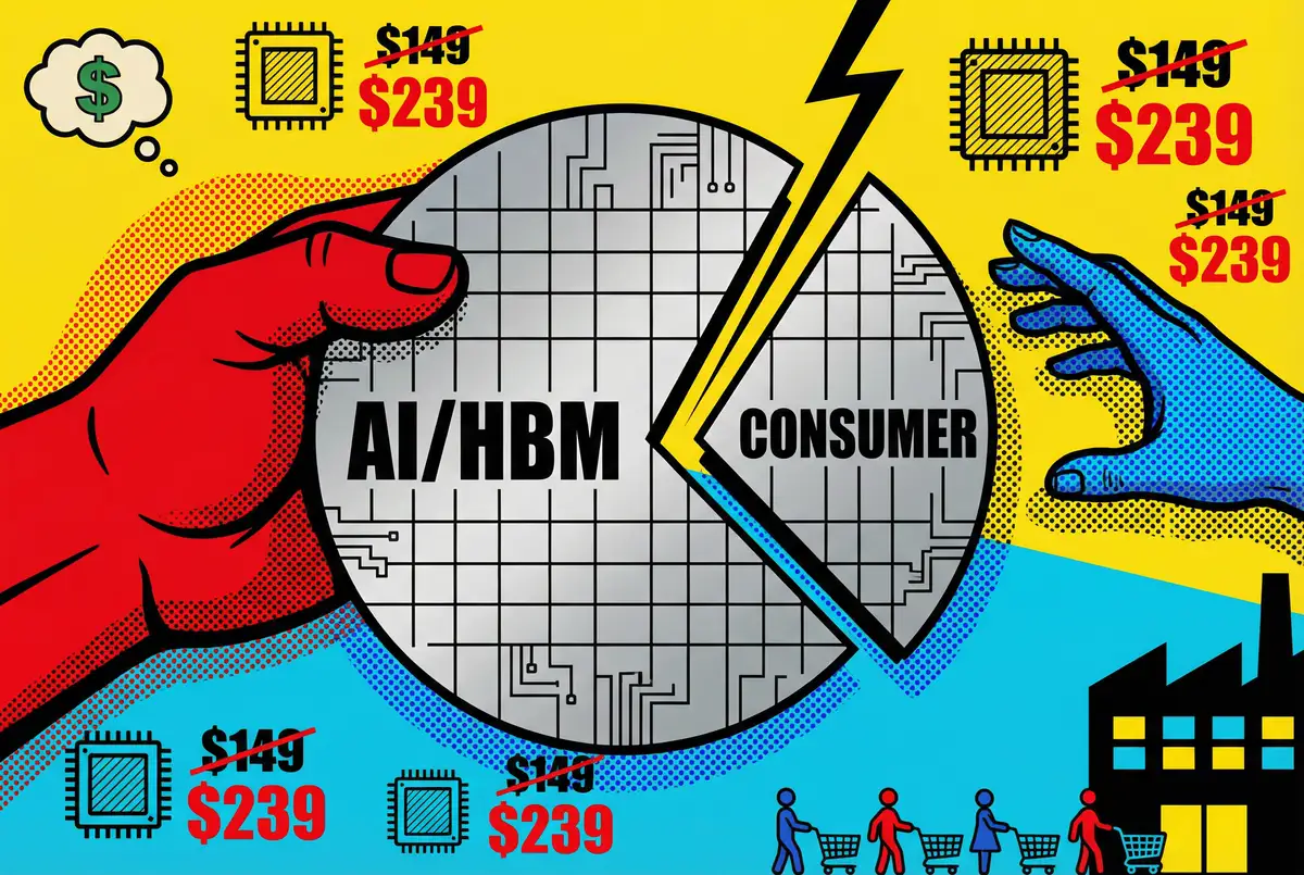
The math matters for an industry straining under AI demand. ASML closed 2025 carrying $39.16 billion in net sales and a backlog that swelled to $46.47 billion. Just the fourth quarter accounted for $16.77 billion in new orders, more than half of it EUV. CEO Christophe Fouquet attributed the surge to stronger expectations for durable AI-driven demand from customers.
A 50% throughput increase per machine gives chipmakers like TSMC and Intel more output without building new fab lines. Each one costs north of ten billion dollars and takes years to bring online. You don't break ground on a new facility when you can upgrade the light source in an existing one. ASML already offers "Productivity Enhancement Packages" that retrofit machines in the field, though older NXE:3400 models may face thermal limits that prevent the upgrade.
The road past one kilowatt
Purvis told Reuters the techniques behind the 1,000-watt mark open a path beyond it. "We see a reasonably clear path toward 1,500 watts, and no fundamental reason why we couldn't get to 2,000 watts." Lab tests had already reached 740 watts using the older single-burst method before ASML switched to its dual-burst approach.
For the semiconductor supply chain, the number itself matters less than what it proves. ASML can double droplet rates and add laser pulses without wrecking the machine's vacuum environment or contaminating the optics. The same engineering logic scales further. Two thousand watts would cut exposure times and push wafer counts higher, and the cost per chip drops with every watt gained. A single EUV machine costs several hundred million euros. Fabs book them years out. At those prices, every percentage point of throughput matters.
ASML proved the system works under customer conditions at its San Diego facility. But a demo that hits 1,000 watts and a machine that holds 1,000 watts for five years on a factory floor are different things. ASML's $46 billion backlog says its customers are betting the company can close that gap.
Frequently Asked Questions
How does ASML's EUV light source actually work?
ASML's machines fire 50,000 molten tin droplets per second through a vacuum chamber. A CO2 laser blasts each droplet, heating the tin into plasma hotter than the sun's surface. That plasma emits extreme ultraviolet light at 13.5 nanometers. Carl Zeiss optics then focus this light onto silicon wafers to print chip features just a few dozen atoms wide.
What changed in the new 1,000-watt system?
Two things. ASML doubled the tin droplet rate from 50,000 to 100,000 per second and added a second laser shaping burst per droplet. These changes pushed the light source from 600 watts to 1,000 watts, a 67% increase. Lab tests had already hit 740 watts with the older single-burst method.
Who is trying to compete with ASML in EUV lithography?
US startups Substrate and xLight have raised hundreds of millions. xLight received about $150 million in Trump administration funding. Substrate uses a particle accelerator to generate shorter-wavelength X-rays. China is also building domestic lithography equipment after being blocked from buying ASML machines. None have shipped a production-ready system.
Why does more EUV power mean more chips?
Higher power shortens exposure times. Chips are printed when EUV light hits photosensitive material on silicon wafers. Brighter light means each wafer spends less time under the beam. ASML projects 330 wafers per hour at 1,000 watts versus 220 today, a 50% gain without building new cleanrooms.
How far can ASML push EUV light source power?
ASML's lead technologist Michael Purvis told Reuters the company sees a clear path to 1,500 watts and no fundamental barrier to 2,000 watts. The dual-burst technique that enabled 1,000 watts could scale further. ASML has also filed patents for a three-burst laser sequence.

Maria Garcia
Bilingual tech journalist slicing through AI noise at implicator.ai. Decodes digital culture with a ruthless Gen Z lens—fast, sharp, relentlessly curious. Bridges Silicon Valley's marble boardrooms, hunting who tech really serves.