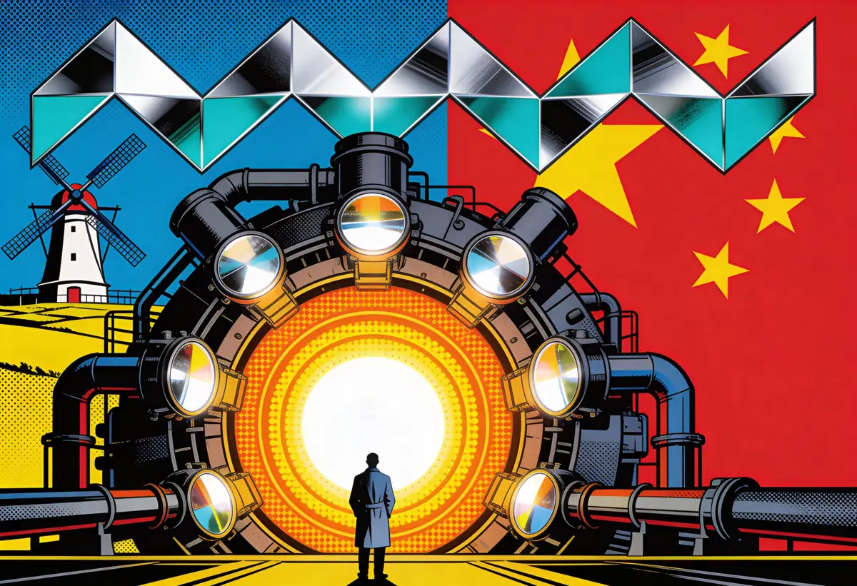
Reuters reported this week that Chinese scientists have assembled a working prototype of an extreme ultraviolet lithography machine inside a high-security Shenzhen lab. The prototype generates EUV light. It sprawls across an entire factory floor. Former ASML engineers built it by reverse-engineering Dutch technology and sourcing components from secondary markets.
What the machine hasn't done is produce a single working chip.
That gap, between generating light and manufacturing semiconductors, contains the entire question of whether export controls have failed or merely been delayed. The distinction matters enormously for policymakers, chipmakers, and the companies whose stock prices dropped 4-5% on the news. It also matters for anyone trying to understand what China has actually accomplished versus what remains aspirational.
Quick Summary
• Reuters reports China completed an EUV prototype in early 2025 using former ASML engineers and $47.5 billion in state funding
• The machine generates EUV light but hasn't produced working chips; ASML took 18 years from prototype to commercial production
• Dutch intelligence warned of talent recruitment after key engineers had already left; European privacy laws limited tracking
• China targets 7nm-5nm nodes by 2028-2030 while ASML ships High-NA systems for 2nm, widening the capability gap
What Reuters Actually Established
Reuters based its story on anonymous sources describing a six-year push that culminated in the prototype earlier this year. Vice Premier Ding Xuexiang reportedly oversees the broader semiconductor strategy. Huawei handles coordination, linking state research institutes with private companies. Thousands of engineers across the country.
Sources described it as China's Manhattan Project. The resource mobilization supports the comparison: Phase III of China's Integrated Circuit Industry Investment Fund launched in May 2024 with 344 billion yuan ($47.5 billion), making it the largest semiconductor investment vehicle in history. The Manhattan Project produced a working weapon. China's prototype has produced light.
Some operational details are striking. Engineers received identification cards under false names and were instructed to use aliases inside the secure facility. Recently retired Chinese-born ASML engineers were prime recruitment targets, offered signing bonuses starting at $420,000 to $700,000 plus housing subsidies. Lin Nan, ASML's former head of light source technology, now works at the Chinese Academy of Sciences' Shanghai Institute of Optics, where his team has filed eight EUV patents in eighteen months.
Get Implicator.ai in your inbox
Strategic AI news from San Francisco. No hype, no "AI will change everything" throat clearing. Just what moved, who won, and why it matters. Daily at 6am PST.
No spam. Unsubscribe anytime.
The human intelligence operation is real. ASML won an $845 million judgment in 2019 against a former Chinese engineer accused of stealing trade secrets. The defendant filed for bankruptcy and continues operating in Beijing with government support. European privacy laws limit ASML's ability to track former employees. Enforcing non-disclosure agreements across borders has proven effectively impossible.
A Dutch Security Failure
If Reuters' reporting holds, this story is as much about Western counterintelligence failure as Chinese capability. ASML sits in Veldhoven, a Dutch town of 45,000 people that happens to host one of the most strategically valuable technology monopolies on the planet. Protecting that monopoly was supposedly someone's job.
Dutch intelligence warned in an April report that China "used extensive espionage programmes" to obtain advanced technology, including recruiting Western scientists and high-tech company employees. The warning came years after the recruitment had already succeeded. Lin Nan left ASML. Other engineers followed. Signing bonuses flowed. Patents accumulated at Chinese research institutes. The April report described a problem that had already spread across institutions and borders.
ASML's internal security measures proved inadequate against a nation-state recruitment operation. The company told Reuters it "vigilantly guards" trade secrets and ensures only select employees can access sensitive information. That compartmentalization didn't prevent engineers from carrying institutional knowledge across borders. You can restrict document access. You cannot erase what someone learned over a career.
The Dutch Ministry of Defence now says the Netherlands is developing policies requiring institutions to perform personnel screenings. The response arrives after the talent has departed, after the patents have been filed, after the prototype has been built. European privacy laws, designed to protect individual rights, created operational space for a systematic talent extraction campaign. The tradeoff was never explicitly debated because nobody anticipated a recruitment operation at this scale.
ASML's $845 million judgment against a single engineer demonstrated legal capacity and practical impotence simultaneously. The defendant filed for bankruptcy. He continues operating in Beijing. Chinese government support shields him from consequences. Every former ASML employee considering a recruitment offer now has a data point: the legal risk is manageable, the financial reward substantial.
This represents a structural failure across Dutch government and corporate security. ASML held a monopoly worth protecting. The Dutch intelligence services understood the threat. Neither mounted an adequate response. The prototype in Shenzhen is built partly from that failure.
The talent pipeline runs deeper than any single company. CSET, the Georgetown security research center, estimated in 2022 that roughly one in ten Chinese semiconductor workers trained overseas. That flow has been underway for years, largely invisible until the capabilities started showing up in Shenzhen.
How EUV Lithography Machines Work
Extreme ultraviolet lithography uses light with a wavelength of 13.5 nanometers to carve circuit patterns onto silicon wafers. That's roughly 14 times shorter than the 193-nanometer light used in older systems, enabling transistors small enough to pack billions onto a chip the size of a fingernail.
Generating the light: A high-power laser fires at tiny droplets of molten tin, 50,000 times per second. Each droplet vaporizes into plasma at 200,000°C, which emits EUV radiation at exactly the wavelength needed. The process requires roughly one megawatt of input power to produce 200 watts of usable EUV light. That's 0.02% efficiency.
Guiding the light: EUV radiation is absorbed by nearly all materials, including air. The entire optical path operates in a vacuum. Multilayer mirrors made of molybdenum and silicon bounce the light toward the wafer. Each mirror reflects only about 70% of incoming photons, so precision compounds across every surface.
Creating the pattern: The focused EUV beam passes through a photomask containing the circuit design, then hits a silicon wafer coated with photoresist. Where light strikes, the chemical degrades, leaving the circuit pattern etched into the surface. A single chip may require over 100 exposure passes.
The machine itself: ASML's EUV systems weigh nearly 200 tons, cost $180-400 million each, and require 1,600 liters of cooling water per minute. Only about 90 exist worldwide. The company spent 18 years and billions of euros moving from prototype to commercial production.
The Technical Gap Nobody Wants to Discuss
ASML had a working EUV prototype in 2001. First commercial chips? 2019. That's eighteen years of iteration, billions of euros burned, careers spent debugging systems that kept failing in new ways.
Beijing's target is 2028. Insiders say 2030 is closer to reality. Either way, we're talking three to five years from prototype to production.
The existence of commercial EUV means Chinese engineers aren't pioneering unknown physics. They can study working machines and build on documented research. But the physics of light generation were never the hard part. ASML understood the physics early. The eighteen-year grind was precision engineering at scales where tiny deviations destroy everything.
The operating temperatures alone should give pause. Tin droplets hit by laser pulses become plasma at 200,000 degrees Celsius. Ten times hotter than the sun's surface, repeated 50,000 times every second. ASML figured out how to make this work reliably. That took most of two decades.
EUV light emerges from that plasma and bounces toward the wafer through a series of mirrors. Here's where ASML's real advantage lives. Those mirrors, stacked layers of molybdenum and silicon, lose about 30% of incoming photons at each surface. After several bounces, most of your light is gone. Zeiss polishes each mirror for months. China's Changchun Institute is trying to replicate that precision. The prototype works, but sources say the optics need "significant refinement."
Power consumption tells you how hard this is. ASML machines draw a megawatt to deliver 200 watts at the wafer. Do the math: 0.02% efficiency. Cooling alone requires 1,600 liters of water every minute. You cannot scale your way past these constraints with a larger footprint.
Size as a Tell
ASML's most advanced EUV systems are roughly the size of a school bus and weigh 180 tons. After failed attempts to replicate that form factor, China's prototype became many times larger, filling an entire factory floor.
This detail reveals more than the sources likely intended. Miniaturization in semiconductor equipment isn't aesthetic preference. It reflects mastery over tolerances, thermal management, and precision alignment. A machine that generates EUV light is an achievement. A machine that generates EUV light while maintaining nanometer-scale precision across thousands of exposures per hour, while managing 200,000-degree plasma, while cooling a system that requires 1,600 liters of water per minute, is a different category of engineering.
The Chinese approach reportedly uses laser-induced discharge plasma rather than ASML's laser-produced plasma technique. Research from Harbin Institute of Technology, which developed the LDP system, suggests this offers advantages in energy efficiency and simplified architecture. Whether those theoretical advantages translate to production-grade reliability remains untested.
The Supply Chain Question
Export controls aimed to deny China access to EUV technology. No ASML EUV system has ever been sold to a Chinese customer. But the controls created unintended consequences.
Older ASML equipment continues circulating through secondary markets. Alibaba Auction sold ASML lithography equipment as recently as October 2025. International banks regularly auction older semiconductor fabrication equipment. Networks of intermediary companies mask ultimate buyers.
Sources say the prototype contains export-restricted components from Japan's Nikon and Canon. Neither company would confirm. Japan's embassy in Washington? No response.
Inside the Shenzhen facility, about 100 recent university graduates spend their days taking apart lithography components, both EUV and older DUV machines. Cameras record each desk. The footage documents every disassembly and reassembly attempt. Get a component back together correctly, you get a bonus.
The operation suggests determination and resources. It doesn't suggest a shortcut around the fundamental engineering challenges that took ASML two decades to solve.
What Would Success Actually Mean?
Say China gets working chips from domestic EUV equipment by 2030. Then what?
The immediate effect would be strategic, not commercial. ASML machines crank out 170-plus wafers per hour at nanometer precision. A prototype spitting test wafers in a lab? Different universe from a production tool pulling three shifts at a commercial fab. Only about 90 EUV systems exist worldwide. That scarcity reflects how hard this technology is to build, and how much leverage it confers.
TSMC, Intel, Samsung have all spent years tuning their processes around ASML's specific performance quirks. Chinese chipmakers would need to develop that expertise from scratch while simultaneously debugging equipment that's generations behind. Process engineering doesn't wait politely for hardware to mature. The timelines run in parallel.
But strategic value isn't about competing commercially. It's about independence. If China can make advanced chips on wholly domestic equipment, even with worse yields and higher costs, the leverage baked into export controls starts evaporating. A $250 million ASML machine matters less than the dependency it creates.
The question becomes whether "meaningful progress," as SemiAnalysis analyst Jeff Koch described it, translates to "sufficient progress" for China's strategic purposes. A domestic chip industry operating at 2024 ASML capability levels by 2030 would still lag the cutting edge. It might be enough.
The Huawei Dimension
Huawei's role extends beyond coordination. The company is involved in every step of the supply chain from chip design and fabrication equipment to manufacturing and final integration into products. CEO Ren Zhengfei reportedly briefs senior Chinese leaders on progress.
Employees assigned to semiconductor teams often sleep on-site and cannot return home during the work week. Phone access is restricted for teams handling sensitive tasks. Teams are deliberately isolated from each other. Few employees know the full scope of the effort.
That kind of operational intensity suggests both commitment and desperation. Huawei landed on the U.S. entity list in 2019. No business with American companies without a license. The restrictions have choked advanced chip production, hobbled smartphone competitiveness. For Huawei, this isn't some abstract national priority. It's survival.
What Remains Unknown
Reuters got impressive operational detail. Technical specs? Much thinner. Nobody's saying what resolution the prototype achieves. Defect rates are a mystery. Throughput relative to commercial systems? Unclear. Whether the machine can hold precision across extended runs, hours of continuous operation, nobody seems to know. Or nobody's telling.
Those gaps matter because EUV light generation is table stakes, not the finish line. The physics work. Engineering determines whether you've got a lab demo or something that could actually run production.
ASML CEO Christophe Fouquet said in April that China would need "many, many years" to develop EUV technology. The company told Reuters that replicating its technology "is no small feat." Both statements remain accurate even if China's prototype generates light on schedule.
Sign up for Implicator.ai
Strategic AI news from San Francisco. Clear reporting on power, money, and policy. Delivered daily at 6am PST.
No spam. Unsubscribe anytime.
The Policy Implications
Export controls did what they were designed to do: no Chinese company runs commercial EUV equipment. But the controls couldn't stop China from throwing resources at the problem, poaching talent, building a prototype.
Whether that counts as failure depends on what you thought controls would accomplish. Nobody serious believed permanent denial was possible. Delay, though. Force China to spend billions while accepting inferior results as Western fabs pushed further ahead. That was achievable. And roughly what happened.
The Trump administration says it's tightening enforcement, working with allies to plug gaps. Fair enough. But the talent already left the Netherlands. The secondary-market components already shipped to Shenzhen. Policy responses now address vulnerabilities that were exploited years ago.
Harder questions come next. Locking down secondary equipment sales means policing a sprawling network of auction houses and resellers across multiple continents. Stopping talent recruitment means accepting that engineers will chase the best paychecks. Staying ahead means funding next-generation R&D while rivals dissect your current machines.
ASML isn't standing still. High-NA systems with 0.55 numerical apertures are shipping to leading fabs. The TWINSCAN EXE:5000 targets 2-nanometer nodes. Meanwhile, China's prototype aims to stabilize production at 7nm or 5nm, nodes that TSMC mastered years ago.
The gap isn't just policy intent. It's measurable in optical resolution: 8nm for High-NA EUV versus an undemonstrated capability from a machine that fills a factory floor. China built a prototype. The distance to the cutting edge keeps growing.
❓ Frequently Asked Questions
Q: Why can't China just buy EUV machines from ASML?
A: U.S. pressure blocked sales starting in 2018, with formal export controls expanding in 2022. No EUV system has ever been sold to a Chinese customer. The restrictions also cover older DUV lithography machines, aiming to keep China at least one generation behind in chipmaking. This forced China to attempt building its own.
Q: What's the difference between China's LDP and ASML's LPP approach?
A: ASML uses laser-produced plasma (LPP), firing lasers at tin droplets to create EUV light. China's Harbin Institute developed laser-induced discharge plasma (LDP), which vaporizes tin between electrodes using high-voltage discharge. LDP reportedly offers simpler architecture and better energy efficiency, but whether it can match LPP's production reliability remains unproven.
Q: What chips can China already make without EUV?
A: Using older DUV lithography with multi-patterning techniques, SMIC produces chips at 7nm for Huawei's Kirin processors. This process is slower and more expensive than EUV. EUV becomes essential for nodes below 7nm, where DUV multi-patterning becomes impractical. TSMC, Intel, and Samsung all require EUV for their most advanced chips.
Q: Why is Carl Zeiss critical to EUV technology?
A: Zeiss manufactures the multilayer mirrors that guide EUV light to the wafer. Each mirror loses about 30% of photons per bounce, so precision is critical. Zeiss spends months polishing each mirror to atomic-level smoothness. China's Changchun Institute is developing alternatives, but sources say their optics still need "significant refinement."
Q: How many EUV machines exist worldwide?
A: Approximately 90 EUV systems operate globally, all built by ASML. Each machine costs $180-400 million, with the newest High-NA systems exceeding $400 million. TSMC, Samsung, and Intel are the primary customers. The scarcity reflects both the technology's difficulty and ASML's production constraints, currently around 50-60 machines per year.
Q: Why is China's prototype so much larger than ASML's machines?
A: ASML's EUV systems are about the size of a school bus and weigh 180 tons. China's prototype fills an entire factory floor. The size difference signals an engineering gap. Miniaturization requires mastery over tolerances, thermal management, and precision alignment. Building larger compensates for lower precision but creates new problems with heat dissipation and component integration.
Q: How is China getting restricted components for the prototype?
A: Through secondary markets and intermediary networks. Alibaba Auction sold ASML lithography equipment as recently as October 2025. International banks regularly auction older fab equipment. Components from Japan's Nikon and Canon, both export-restricted, reportedly ended up in the prototype. Networks of intermediary companies mask ultimate buyers, making enforcement difficult.
Q: What would China need to prove before this prototype matters commercially?
A: Three things: resolution (can it etch patterns fine enough for advanced chips), throughput (can it process enough wafers per hour to be economical), and reliability (can it maintain precision across extended production runs). ASML machines expose 170-plus wafers hourly at nanometer precision. China's prototype hasn't demonstrated any of these metrics publicly.

Marcus Schuler
Tech translator with German roots who fled to Silicon Valley chaos. Decodes startup noise from San Francisco. Launched implicator.ai to slice through AI's daily madness—crisp, clear, with Teutonic precision and sarcasm. E-Mail: [email protected]